![]()
![]()
![]()
![]()
![]()
Research Support Office Research Advancement Division. Tokyo University of Agriculture and Technology
| TEL | +81-42-367-5944 |
|---|---|
| FAX | +81-42-367-5946 |
This program is supported by MEXT’s scientific technology human resource development fee grant, "Program to Disseminate Tenure Tracking System".
![]()


Home > Tenured Faculties > Murakami Hisashi

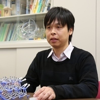
Murakami Hisashi
| Affiliation | Institute of Engineering |
|---|---|
| Division | Division of Applied Chemistry |
| Research field | Crystal engineering,Crystal growth |
| Keyword(S) | Epitaxial growth,III-Nitride semiconductors |
| Url | http://murakamilab.jpn.org/ |
| Research experience | ・Oct.2003-Mar.2005:Research Fellowship for Young Scientists (DC2), Japan Society for the Promotion of Science |
|---|---|
| Educational background | ・Apr.1996-Mar.2000:Bachelor of Engineering, Tokyo University of Agriculture and Technology |
| Awards | * The latest information is shown at the member's website. |
| Selected papers and publications | * The latest information is shown at the member's website. |
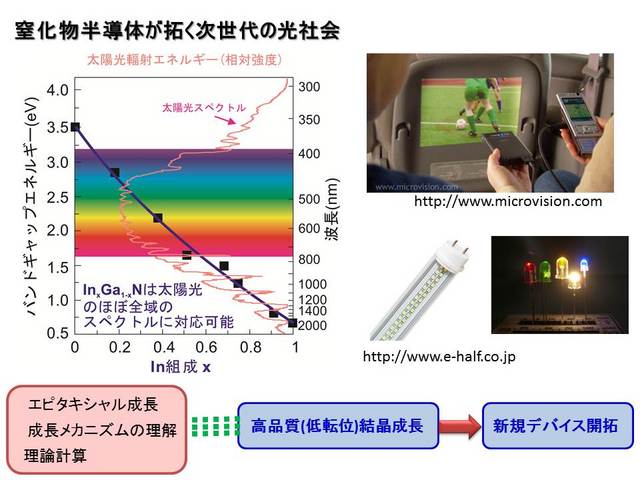
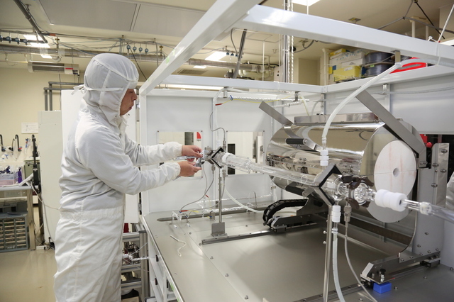
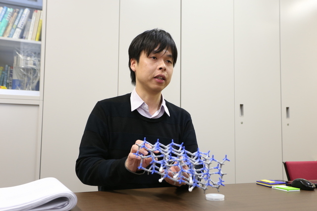
The requirements to power and energy saving are ignited with recent big earthquake and Fukushima nuclear power plant disasters as a trigger. III-nitride semiconductors, which are key materials for the realization of next-generation optoelectronic devices and construction of low carbon society, are promising for the optical devices operated from deep UV to near infrared regions because of their bandgaps (AlN: 6.2eV, GaN: 3.4eV, InN: 0.7eV). Recently, light emitting diodes (LEDs) of 282nm, which can be used for sterilization, and 210nm (shortest wavelength in nitride-LEDs) were demonstrated. Also, a green laser diodes (LDs) emitted at 534nm with continuous operation was realized in Japanese company. However, there are little reports on light emitters operated at pure green or longer wavelength region. This is because it is quite difficult to obtain a high In content over 20% of InxGa1-xN, which is used as active layer in LEDs, and recombination probability between electrons and holes are significantly decreased due to the internal and piezoelectric fields originated from asymmetric crystal structure. Therefore, fabrication of device structures on non-polar or semi-polar direction is attempted in recent years. Henceforth, it is desperately needed to grow high quality In-related nitride semiconductor crystals and non-polar GaN thick crystals for the realization of light receiving and light emitting devices operated at unexplored wavelength region. I plan to solve these problems by two approaches as follows. 1. Growth of high quality and thick InxGa1-xN alloy by halide vapor phase epitaxy (HVPE), 2. Establishment of growth technology on non-polar nitride semiconductors.
The tenure track system is very effective for a young researcher because the environments of independent research laboratory and devoting his research activity are put into place. In this tenure track project, TUAT has received quite high evaluation to the past five years endeavor. I'm very honored that I can participate in this project as an member for 5 years from now on.
III-nitride semiconductors are very important materials for overcoming the future energy issue in the world by next-generation white general lighting, high-efficiency solar cells and power devices for automobile. I will proceed my research from the viewpoint of the control of crystal growth in atomic-level and the feedback from the mechanism of crystal growth.


![]()